- 您现在的位置:买卖IC网 > Sheet目录368 > W25Q128BVEIG (Winbond Electronics)IC SPI FLASH 128MBIT 8WSON
�� �
�
�W25Q128BV�
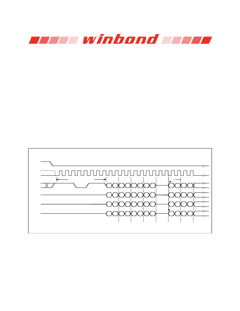
�7.2.16� Word� Read� Quad� I/O� (E7h)�
�The� Word� Read� Quad� I/O� (E7h)� instruction� is� similar� to� the� Fast� Read� Quad� I/O� (EBh)� instruction� except�
�that� the� lowest� Address� bit� (A0)� must� equal� 0� and� only� two� Dummy� clocks� are� required� prior� to� the� data�
�output.� The� Quad� I/O� dramatically� reduces� instruction� overhead� allowing� faster� random� access� for� code�
�execution� (XIP)� directly� from� the� Quad� SPI.� The� Quad� Enable� bit� (QE)� of� Status� Register-2� must� be� set� to�
�enable� the� Word� Read� Quad� I/O� Instruction.�
�Word� Read� Quad� I/O� with� “Continuous� Read� Mode”�
�The� Word� Read� Quad� I/O� instruction� can� further� reduce� instruction� overhead� through� setting� the�
�“Continuous� Read� Mode”� bits� (M7� -0)� after� the� input� Address� bits� (A23-0),� as� shown� in� Figure� 15a.� The�
�upper� nibble� of� the� (M7-4)� controls� the� length� of� the� next� Fast� Read� Quad� I/O� instruction� through� the�
�inclusion� or� exclusion� of� the� first� byte� instruction� code.� The� lower� nibble� bits� of� the� (M3-� 0)� are� don’t� care�
�(“x”).� However,� the� IO� pins� should� be� high� -impedance� prior� to� the� falling� edge� of� the� first� data� out� clock.�
�If� the� “Continuous� Read� Mode� ”� bits� M5-4� =� (1,0),� then� the� next� Fast� Read� Quad� I/O� instruction� (after� /CS�
�is� raised� and� then� lowered)� does� not� require� the� E7h� instruction� code,� as� shown� in� Figure� 15b.� This�
�reduces� the� instruction� sequence� by� eight� clocks� and� allows� the� Read� address� to� be� immediately� entered�
�after� /CS� is� asserted� low.� If� the� “Continuous� Read� Mode� ”� bits� M5-4� do� not� equal� to� (1,0),� the� next�
�instruction� (after� /CS� is� raised� and� then� lowered)� requires� the� first� byte� instruction� code,� thus� returning� to�
�normal� operation.� A� “Continuous� Read� Mode”� Reset� instruction� can� also� be� used� to� reset� (M7� -0)� before�
�issuing� normal� instructions� (See� 7.2.20� for� detail� descriptions).�
�/CS�
�Mode� 3�
�0�
�1�
�2�
�3�
�4�
�5�
�6�
�7�
�8�
�9�
�10�
�11�
�12�
�13�
�14�
�15�
�16�
�17�
�18�
�19�
�20�
�21�
�CLK�
�Mode� 0�
�Instruction� (E7h)�
�A23-16�
�A15-8�
�A7-0�
�M7-0�
�Dummy�
�IOs� switch� from�
�Input� to� Output�
�IO� 0�
�IO� 1�
�IO� 2�
�IO� 3�
�20�
�21�
�22�
�23�
�16�
�17�
�18�
�19�
�12�
�13�
�14�
�15�
�8�
�9�
�10�
�11�
�4�
�5�
�6�
�7�
�0�
�1�
�2�
�3�
�4�
�5�
�6�
�7�
�0�
�1�
�2�
�3�
�4�
�5�
�6�
�7�
�0�
�1�
�2�
�3�
�4�
�5�
�6�
�7�
�0�
�1�
�2�
�3�
�4�
�5�
�6�
�7�
�Byte� 1�
�Byte� 2�
�Byte� 3�
�Figure� 15a.� Word� Read� Quad� I/O� Instruction� Sequence� (Initial� instruction� or� previous� M5-4� ?� 10)�
�-� 34� -�
�发布紧急采购,3分钟左右您将得到回复。
相关PDF资料
W25Q16BVSFIG
IC SPI FLASH 16MBIT 16SOIC
W25Q16CVSFIG
IC SPI FLASH 16MBIT 16SOIC
W25Q16DWSFIG
IC FLASH SPI 16MBIT 16SOIC
W25Q16VSFIG
IC FLASH 16MBIT 80MHZ 16SOIC
W25Q32BVZPIG
IC SPI FLASH 32MBIT 8WSON
W25Q32DWZEIG
IC FLASH SPI 32MBIT 8WSON
W25Q40BWSSIG
IC FLASH SPI 4MBIT 8SOIC
W25Q40BWZPIG
IC FLASH SPI 4MBIT 8WSON
相关代理商/技术参数
W25Q128BVEIG TR
制造商:Winbond Electronics Corp 功能描述:SPIFLASH, 128M-BIT, 4KB UNIFOR
W25Q128BVEIP
制造商:WINBOND 制造商全称:Winbond 功能描述:3V 128M-BIT SERIAL FLASH MEMORY WITH DUAL AND QUAD SPI
W25Q128BVFIG
制造商:Winbond Electronics Corp 功能描述:Flash Serial-SPI 3.3V 128Mbit 16M x 8bit 8.5ns 16-Pin SOIC 制造商:Winbond Electronics Corp 功能描述:128MB SPI FLASH
W25Q128BVFIP
制造商:WINBOND 制造商全称:Winbond 功能描述:3V 128M-BIT SERIAL FLASH MEMORY WITH DUAL AND QUAD SPI
W25Q128FV
制造商:WINBOND 制造商全称:Winbond 功能描述:SERIAL FLASH MEMORY WITH DUAL/QUAD SPI & QPI
W25Q128FVAIG
制造商:WINBOND 制造商全称:Winbond 功能描述:3V 128M-BIT SERIAL FLASH MEMORY WITH DUAL/QUAD SPI & QPI
W25Q128FVAIP
制造商:WINBOND 制造商全称:Winbond 功能描述:3V 128M-BIT SERIAL FLASH MEMORY WITH DUAL/QUAD SPI & QPI
W25Q128FVAIQ
制造商:WINBOND 制造商全称:Winbond 功能描述:3V 128M-BIT SERIAL FLASH MEMORY WITH DUAL/QUAD SPI & QPI